Pulse Generators
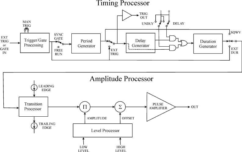
Pulse generators (PGs) are square-wave waveform sources. Square-waves are waveforms with two main levels, high and low. PGs generate square-waves over a range of frequencies, duty ratios, transition times between levels, and values of the levels themselves. The waveforms can be repetitive, single-cycle, or gated. They can be triggered from an external source and can be delayed relative to an external trigger event.
The Innovatia PG projects are listed in the following table. Each column names the PG project and its state of development. Major characteristics are described.
The PG280 and PG201 working prototypes are being adapted to the specifications given below. The PG202 circuit design is completed and ready for a prototype build.
|
PG200
Series |
PG201 |
PG202 |
PG210 |
PG220 |
PG280 |
|
Priority,
phase |
2,
D1 |
1,
C2 |
3,
C0 |
5,
C1 |
4,
D2 |
|
PG
Frequency |
single-pulse |
2
MHz |
10
MHz |
20
MHz |
single-pulse |
|
Trig/Gate
Proc. |
μC-driven |
gate |
BJT
array |
BJT
array |
μC-driven |
|
Period
Gen. |
μC-driven |
Gate-based
AST 3
ranges mpyr
I source |
50 MHz
16-bit DDS |
15
ns GAL 8-bit 40 MHz NCO with range prescaler |
μC-driven |
|
Delay
Gen |
μC-driven |
none |
DDS includes PWM overlapping or non-overlapping push-pull gate-drive waveforms |
Delay & PWM overlapping or non-overlapping push-pull gate-drive waveforms |
μC-driven |
|
Duration
Gen. |
μC-driven |
Gate-based RC MST; 3 ranges |
50 MHz
16-bit DDS |
40
MHz down cntr |
μC-driven |
|
Transition
Proc. |
none |
none |
Analog |
Analog |
none |
|
Level
Proc. |
0 V
to DAC level |
LM13700 |
High-
and low-level DACs |
LM1496 dual
2Q mpyr |
C-bank
selection |
|
Pulse
Amplifier |
OUT
Port: 30 V, 5 A; 2-range, 3 dec V
or I out; isolation
amplifiers |
±20 V
open, 50 Ω out Discrete
BJTs |
dual,
±10 V
open, 50 Ω
out; level-switched |
±10 V
open, active
50 Ω out LM3161 |
800
V 250
A 200
kW (pulsed) isolated |
|
Power
Supply |
12 V,
0.25 A 0.2 A
C-bank charger |
12 V,
1.25 A in 5
V, 0.12 A ±12 V,
50 mA ±24
V, 215 mA 15
W |
5
V, 250 mA ±12
V, 250 mA 10
W |
5
V, 250 mA ±12
V, 250 mA 10
W |
Charger
input: power-line 165 V
dc, 5 A rms ±12
V, 0.1 A 5
V, 0.2 A |
|
μC |
MC2
prototype, ATmega328 |
MC2
prototype, ATmega328 |
ATmega328 |
ATmega328 |
ATmega328 |
|
Front-Panel |
FP1
+ 4sw +
digiknob |
FP1
+ 4sw +
digiknob |
4-digit
LED, 4sw + digiknob |
4-digit
LED, 4sw + digiknob |
Serial
port (SCI) |
|
Notes |
PG3-derived
Power SMU |
analog
timing ±20 V
output |
μC-based
timing |
PLD
DDS timing |
Transient-discharge
SMU |
The design goal for the minimum transition times for PGs (risetime, falltime) is that they be 15% or less the minimum pulse period. For a maximum pulse frequency of 10MHz, the period is 100ns and the transition time design goal is that they be less than 15 ns. The design goal for pulse transition overshoot < 5%.
The PG201 analog circuit subsystem is at Prototype Release but the computer and user interface (digital subsystem) are in design phase.
The PG280 analog subsystem is undergoing some modification from a design that has achieved Prototype Release for a somewhat different application. The digital subsystem is in design phase.
FP1 is a 16-character LCD display.
Innovatia Assistants: inquire for project documentation and ECBs.
![]()
![]()
![]()
![]()
![]()